
《德源科技》r)L3GD20 3-Axis Gyro Carrier with Voltage Regulator
PI2125
$1,053
已售出 2 件
運費抵用券全家訂單滿$99運費折抵10元
- 現金付款
- 全家取貨付款
現金付款
- Yahoo奇摩輕鬆付現金接受付款方式:ATM轉帳 / Famiport / 輕鬆付帳戶餘額
ATM 提供5家銀行:合作金庫、華南銀行、台灣銀行、國泰世華、中國信託,以上5家同行轉帳,免轉帳手續費。
全家取貨付款
— Yahoo奇摩輕鬆付全家取貨付款 — 單件運費$60
郵局掛號 — 單件運費$60

輕鬆付提供價金保管,交易更安心!
商品資訊
下標前請注意: (請先打電話連絡或提問,請見賣方關於我中有聯絡方式)
1.可以開發票
(PS:如合併結帳多項產品或是加購附件及開發票者,使用全家取貨付款的,結標後請自行修改金額)
2.可面交,現貨供應
3.下標後請填寫下列資料
1.帳號:
2.購買物品名稱:(如有很多型號時請註明清楚,謝謝)
3.地址:
4.郵遞區號:
5.郵款金額:
6.姓名:
7.帳號後5碼:
8.連絡電話:
===================================================================
id=6311
※本產品原廠代理從國外進口,有些交期較長,下訂前請詢問!

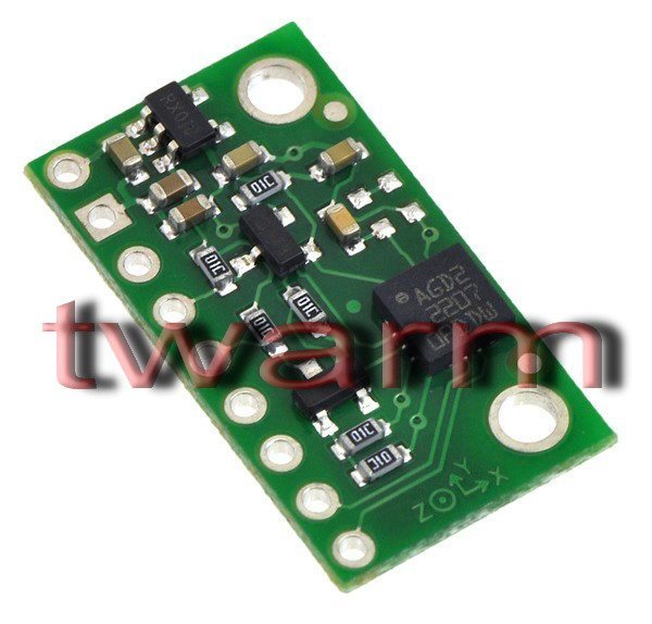
L3GD20 3-Axis Gyro Carrier with Voltage Regulator
This sensor is a carrier/breakout board for the ST L3GD20 three-axis gyroscope, which measures the angular rates of rotation about the pitch (x), roll (y), and yaw (z) axes. Angular velocity measurements with a configurable range of ±250°/s, ±500°/s, or ±2000°/s can be read through a digital I²C or SPI interface. The board has a 3.3 V linear regulator and integrated level-shifters that allow it to work over an input voltage range of 2.5–5.5 V, and the 0.1″ pin spacing makes it easy to use with standard solderless breadboards and 0.1″ perfboards.
 |
Overview
This board is a compact (0.5″ × 0.9″) breakout board for ST’s L3GD20 three-axis digital-output gyroscope; we therefore recommend careful reading of the L3GD20 datasheet (2MB pdf) before using this product. The L3GD20 is a great IC, but its small, leadless, LGA package makes it difficult for the typical student or hobbyist to use. It also operates at voltages below 3.6 V, which can make interfacing difficult for microcontrollers operating at 5 V. This carrier board addresses these issues by incorporating additional electronics, including a 3.3 V voltage regulator and level-shifting circuits, while keeping the overall size as compact as possible. The board ships fully populated with its SMD components, including the L3GD20, as shown in the product picture.
Compared to the L3G4200D, the L3GD20 uses a higher resonant frequency that makes it more resistant to audio noise and vibrations. This board remains pin-compatible with the original L3G4200D carrier, although changes in I²C addresses and configuration registers mean that code written to interface with an L3G4200D might need to be modified to work with an L3GD20.
The L3GD20 has many configurable options, including three selectable angular rate sensitivities, a choice of output data rates, an embedded FIFO for buffering output data, and a programmable external interrupt signal. The three angular velocity readings are available through a digital interface, which can be configured to operate in either I²C or SPI mode.
The carrier board includes a low-dropout linear voltage regulator that provides the 3.3 V required by the L3GD20, which allows the sensor to be powered from a 2.5-5.5 V supply. The regulator output is available on the VDD pin and can supply almost 150 mA to external devices. The breakout board also includes a circuit that shifts the I²C/SPI clock and data in lines to the same logic voltage level as the supplied VIN, making it simple to interface the board with 5 V systems, and the board’s 0.1″ pin spacing makes it easy to use with standard solderless breadboards and 0.1″ perfboards.
For sensor fusion applications, our MinIMU-9 v2 and AltIMU-10 inertial measurement units combine the L3GD20 with an LSM303DLHC 3-axis accelerometer and 3-axis magnetometer on a single board, providing nine independent readings that can be used to calculate an absolute orientation. The AltIMU-10 also includes an LPS331AP pressure sensor that can be used to calculate altitude.
Specifications
- Dimensions: 0.5″ × 0.9″ × 0.1″ (13 × 23 × 3 mm)
- Weight without header pins: 0.7 g (0.03 oz)
- Operating voltage: 2.5 to 5.5 V
- Supply current: 7 mA
- Output format (I²C/SPI): one 16-bit reading per axis
- Sensitivity range (configurable): ±250°/s, ±500°/s, or ±2000°/s
Included components
A 9×1 strip of 0.1″ header pins and a 9×1 strip of 0.1″ right-angle header pins are included, as shown in the picture below. You can solder the header strip of your choice to the board for use with custom cables or solderless breadboards, or you can solder wires directly to the board itself for more compact installations.
 |
Using the L3GD20
Connections
Regardless of the interface being used to communicate with the L3GD20, its VIN pin should be connected to a 2.5-5.5 V source, and GND should be connected to 0 volts. (Alternatively, if you are using the gyro with a 3.3 V system, you can leave VIN disconnected and bypass the built-in regulator by connecting 3.3 V directly to VDD.)
A minimum of two logic connections are necessary to use the L3GD20 in I²C mode (this is the default mode): SCL and SDA. These should be connected to an I²C bus operating at the same logic level as VIN.
To use the L3GD20 in the default SPI mode, four logic connections are required: SPC, SDI, SDO, and CS. These should be connected to an SPI bus operating at the same logic level as VIN. The SPI interface operates in 4-wire mode by default, with SDI and SDO on separate pins, but it can be configured to use 3-wire mode so that SDO shares a pin with SDI.
|
|


Pinout
| PIN | Description |
|---|---|
| VIN | This is the main 2.5-5.5 V power supply connection. The SCL/SPC and SDA/SDI level shifters pull the I²C and SPI bus high bits up to this level. |
| GND | The ground (0 V) connection for your power supply. Your I²C or SPI control source must also share a common ground with this board. |
| VDD | Regulated 3.3 V output. Almost 150 mA is available to power external components. (If you want to bypass the internal regulator, you can instead use this pin as a 3.3 V input with VIN disconnected.) |
| SCL/SPC | Level-shifted I²C/SPI clock line: HIGH is VIN, LOW is 0 V |
| SDA/SDI | Level-shifted I²C data line and SPI data in line (also doubles as SDO in 3-wire mode): HIGH is VIN, LOW is 0 V |
| SDO | SPI data out line in 4-wire mode: HIGH is VDD, LOW is 0 V. This output is not level-shifted. Also used as an input to determine I²C slave address (see below). |
| CS | SPI enable (chip select). Pulled up to VDD to enable I²C communication by default; drive low to begin SPI communication. |
| DRDY/INT2 | Data ready indicator, a 3.3-V-logic-level output. HIGH (3.3 V) indicates angular rate data can be read. Can also be configured as a FIFO interrupt. This output is not level-shifted. |
| INT1 | Programmable interrupt, a 3.3-V-logic-level output. This output is not level-shifted. |
Schematic Diagram
 |
The above schematic shows the additional components the carrier board incorporates to make the L3GD20 easier to use, including the voltage regulator that allows the board to be powered from a 2.5-5.5 V supply and the level-shifter circuit that allows for I²C and SPI communication at the same logic voltage level as VIN.
I²C Communication
With the CS pin in its default state (pulled up to VDD), the L3GD20 can be configured and its angular velocity readings can be queried through the I²C bus. Level shifters on the I²C clock (SCL) and data (SDA) lines enable I²C communication with microcontrollers operating at the same voltage as VIN (2.5-5.5 V). A detailed explanation of the I²C interface on the L3GD20 can be found in its datasheet (1MB pdf), and more detailed information about I²C in general can be found in NXP’s I²C-bus specification (371k pdf).
In I²C mode, the gyro’s 7-bit slave address has its least significant bit (LSb) determined by the voltage on the SDO pin. The carrier board pulls SDO to VDD through a 10 kΩ resistor, making the LSb 1 and setting the slave address to 1101011b by default. If the gyro’s selected slave address happens to conflict with some other device on your I²C bus, you can drive SDO low to set the LSb to 0.
In our tests of the board, we were able to communicate with the chip at clock frequencies up to 400 kHz; higher frequencies might work but were not tested. The chip itself and carrier board do not meet of some requirements to make the device compliant with I²C fast-mode. It is missing 50 ns spike suppression on the clock and data lines, and additional pull-ups on the clock and data lines might also be necessary to achieve compliant signal timing characteristics.
SPI Communication
To communicate with the L3GD20 in SPI mode, the CS pin (which the board pulls to VDD through a 10 kΩ resistor) must be driven low before the start of an SPI command and allowed to return high after the end of the command. Level shifters on the SPI clock (SPC) and data in (SDI) lines enable SPI communication with microcontrollers operating at the same voltage as VIN (2.5-5.5 V).
In the default 4-wire mode, the gyro transmits data to the SPI master on a dedicated data out (SDO) line. If the SPI interface is configured to use 3-wire mode instead, the SDI line doubles as SDO and is driven by the L3GD20 when it transmits data to the master. A detailed explanation of the SPI interface on the L3GD20 can be found in its datasheet (1MB pdf).
Sample Code
We have written a basic Arduino library for the L3GD20 that makes it easy to interface this sensor with an Arduino. The library makes it simple to configure the L3GD20 and read the raw gyro data through I²C.
Protocol Hints
The datasheet provides all the information you need to use this sensor, but picking out the important details can take some time. Here are some pointers for communicating with and configuring the L3GD20 that we hope will get you up and running a little bit faster:
- The gyro is in power down mode by default. You have to turn it on by writing the appropriate value to the CTRL_REG1 register.
- You can read or write multiple registers in a single I²C command by asserting the most significant bit of the register address to enable address auto-increment.
- You can enable the same auto-increment feature in SPI mode by asserting the second bit (bit 1, called the MS bit in the datasheet) of an SPI command.